S9014LT1
商品详情
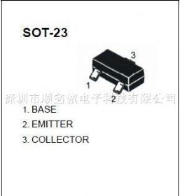
S9014LT1 TRANSISTOR( NPN )
FEATURES
· High total power dissipation.(pc=0.2w)
·Complementary to S9015LT1
MARKING: L6 J6
MAXIMUM RATINGS* TA=25℃ unless otherwise noted
Symbol Parameter Value Units
VCBO Collector-Base Voltage 50 V
VCEO Collector-Emitter Voltage 45 V
VEBO Emitter-Base Voltage 5 V
IC Collector Current -Continuous 0.1 A
PC Collector Dissipation 0.2 W
TJ, Tstg Junction and Storage Temperature -55-150 ℃
ELECTRICAL CHARACTERISTICS(Tamb=25℃ unless otherwise specified)
Parameter Symbol Test conditions MIN TYP MAX UNIT
Collector-base breakdown voltage V(BR)CBO Ic= 100μA, IE=0 50 V
Collector-emitter breakdown voltage V(BR)CEO Ic= 0.1mA, IB=0 45 V
Emitter-base breakdown voltage V(BR)EBO IE=100μA, IC=0 5 V
Collector cut-off current ICBO VCB=50 V , IE=0 0.1 μA
Collector cut-off current ICEO VCE=35V , IB=0 0.1 μA
Emitter cut-off current IEBO VEB= 3V , IC=0 0.1 μA
DC current gain hFE VCE=5V, IC= 1mA 200 1000
Collector-emitter saturation voltage VCE(sat) IC=100 mA, IB= 5mA 0.3 V
Base-emitter saturation voltage VBE(sat) IC=100 mA, IB= 5mA 1 V
Transition frequency fT
VCE=5V, IC= 10mA
f=30MHz
150 MHz
CLASSIFICATION OF hFE(1)
Rank C D
Range 200-400 400-1000