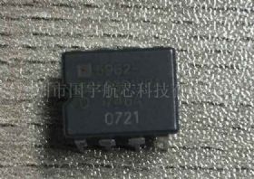

EVX10DS130AGS 订货 13632767652
商品详情
EVX10DS130AGS 订货 13632767652
DAC 1-CH Pipelined 10Bit 255-Pin CI-CGA
The EV10DS130A/B is a 10-bit 3 GSps DAC with an integrated 4:1 or 2:1 multiplexer, allowing easy
interface with standard LVDS FPGAs thanks to user friendly features as OCDS, PSS.
interface with standard LVDS FPGAs thanks to user friendly features as OCDS, PSS.
Key Features
• 10-bit Resolution
• 3 GSps Guaranteed Conversion Rate
• 6 GHz Analog Output Bandwidth
• 60 ps Full Scale Rise Time
• 4:1 or 2:1 integrated Parallel MUX (Selectable)
• Selectable Output Modes for Performance Optimization:
Return to Zero, Non Return to Zero, Narrow Return to Zero, RF
• Low Latency Time: 3.5 Clock Cycles
• 1.4 Watt Power Dissipation in MUX 4:1 Mode
• Functions
– Selectable MUX Ratio 4:1 (Full Speed), 2:1 (Half Speed)
– Triple Majority Voting
– User-friendly Functions:
- Gain Adjustment
- Input Data Check Bit (FPGA Timing Check)
- Setup Time and Hold Time Violation Flags (STVF, HTVF)
- Clock Phase Shift Select for Synchronization with DSP (PSS[2:0])
- Output Clock Division Selection (Possibility to Change the Division Ratio of the DSP Clock)
- Input Under Clocking Mode
- Diode for Die junction Temperature Monitoring
• LVDS Differential Data input and DSP Clock Output
• Analog Output Swing: 1Vpp Differential (100 Differential Impedance)
• External Reset for Synchronization of Multiple MuxDACs
• Power Supplies : 3.3 V (Digital), 3.3V & 5.0V (Analog)
• LGA255, CCGA255, Ci-CGA255 Package (21 × 21 mm Body Size, 1.27 mm Pitch)
• 3 GSps Guaranteed Conversion Rate
• 6 GHz Analog Output Bandwidth
• 60 ps Full Scale Rise Time
• 4:1 or 2:1 integrated Parallel MUX (Selectable)
• Selectable Output Modes for Performance Optimization:
Return to Zero, Non Return to Zero, Narrow Return to Zero, RF
• Low Latency Time: 3.5 Clock Cycles
• 1.4 Watt Power Dissipation in MUX 4:1 Mode
• Functions
– Selectable MUX Ratio 4:1 (Full Speed), 2:1 (Half Speed)
– Triple Majority Voting
– User-friendly Functions:
- Gain Adjustment
- Input Data Check Bit (FPGA Timing Check)
- Setup Time and Hold Time Violation Flags (STVF, HTVF)
- Clock Phase Shift Select for Synchronization with DSP (PSS[2:0])
- Output Clock Division Selection (Possibility to Change the Division Ratio of the DSP Clock)
- Input Under Clocking Mode
- Diode for Die junction Temperature Monitoring
• LVDS Differential Data input and DSP Clock Output
• Analog Output Swing: 1Vpp Differential (100 Differential Impedance)
• External Reset for Synchronization of Multiple MuxDACs
• Power Supplies : 3.3 V (Digital), 3.3V & 5.0V (Analog)
• LGA255, CCGA255, Ci-CGA255 Package (21 × 21 mm Body Size, 1.27 mm Pitch)